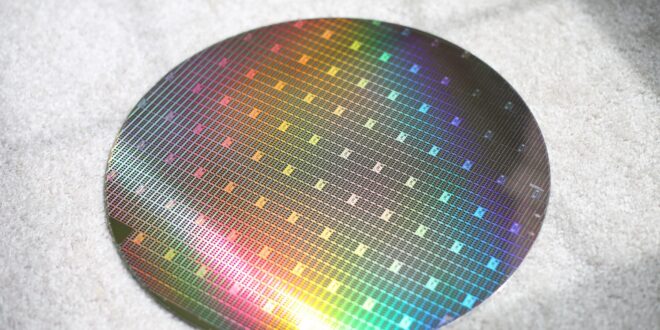
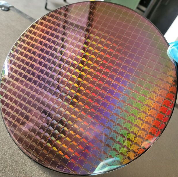
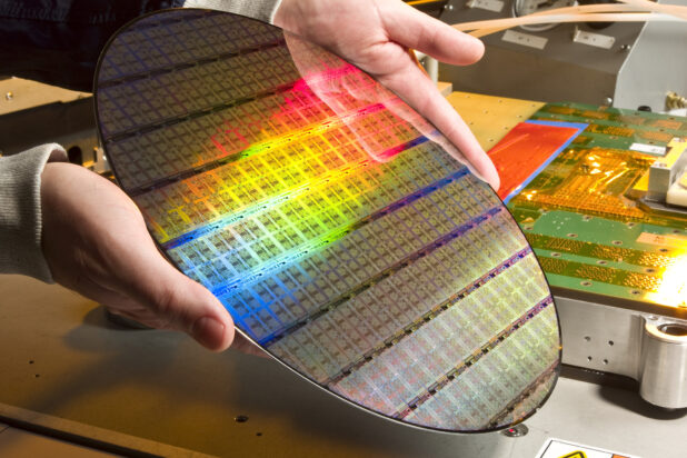
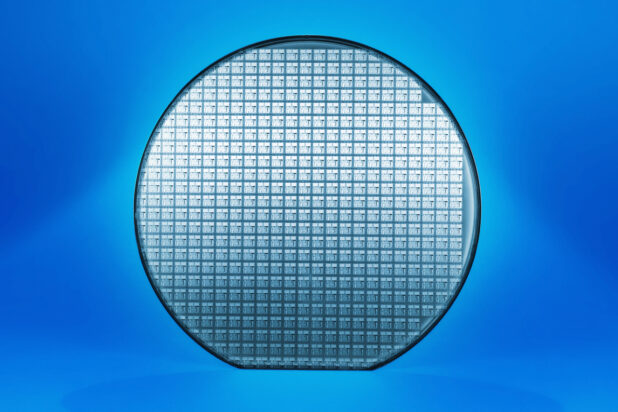
Silicon wafers are the foundation of modern semiconductor devices, serving as the substrate on which intricate electronic components are built. These wafers are typically smooth and feature a uniform structure. However, the advent of patterned silicon wafers has brought about a new era in semiconductor technology, enabling enhanced performance and unlocking a wide range of applications.
Table of Contents
The Basics of Silicon Wafers
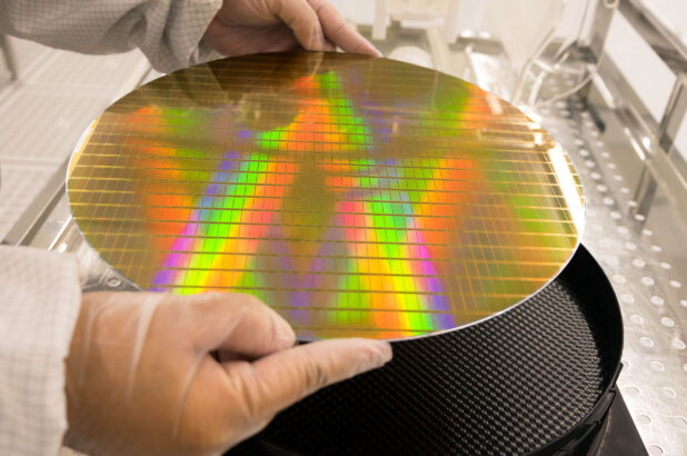
To understand patterned wafers, it is crucial to grasp the basics of silicon wafers themselves. Silicon wafers are thin, round discs typically made from high-purity single-crystal silicon. They are meticulously crafted to exhibit precise electrical properties and structural characteristics. These wafers serve as the backbone for the fabrication of microchips, integrated circuits, and other electronic components.
Understanding Patterns
Patterned silicon wafers introduce intentional modifications to the smooth and uniform surface of traditional wafers. These modifications can take various forms, such as etched patterns, nanoscale structures, or selective doping. The patterns can be designed to enhance specific functionalities, improve performance, or enable unique applications. By strategically altering the surface properties, patterned silicon wafers offer new possibilities for advanced semiconductor devices.
Manufacturing Process
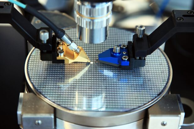
The process of creating patterned silicon wafers begins by carefully selecting a silicon wafer that meets the desired specifications. Once selected, a photoresist material is applied to the wafer’s surface. The photoresist acts as a protective layer that will undergo the patterning process. Lithographic techniques, such as photolithography, are then employed to transfer the desired pattern onto the photoresist-coated wafer. This involves using masks or laser beams to selectively expose the photoresist to light, creating a patterned mask on the wafer.
After the patterning step, the wafer undergoes a series of additional processes to bring the intended structures or modifications to life. Etching techniques, such as wet etching or plasma etching, are employed to remove the exposed or unmasked portions of the wafer’s surface. This etching process selectively removes the material, leaving behind the desired pattern.
Deposition techniques are then used to add additional materials onto the patterned wafer surface. These materials may include metals, insulators, or semiconductors, depending on the specific application. The deposition process can be achieved through various methods like physical vapor deposition (PVD), chemical vapor deposition (CVD), or atomic layer deposition (ALD). The deposited material fills the voids created by the etching process and contributes to the formation of the desired structures.
Doping, another critical step, involves introducing impurities into specific regions of the patterned wafer. This is achieved by applying dopant materials or using ion implantation techniques. Doping alters the electrical properties of the silicon, allowing for the creation of regions with different conductivity types (e.g., n-type or p-type) and enabling the functionality of various electronic devices.
Throughout the entire manufacturing process of patterned silicon wafers, precision, and accuracy are of utmost importance. Each step must be executed with meticulous attention to detail to ensure the final product meets the required specifications. The alignment of masks, the control of etching depths, the uniformity of depositions, and the precise doping profiles all contribute to the overall quality and performance of the patterned silicon wafers. Any deviation or error at any stage can significantly impact the functionality and reliability of the final product.
Fields of application
Patterned silicon wafers have found applications across a wide range of industries. In the field of electronics, they have been instrumental in the development of advanced microprocessors, memory devices, and sensors. Their unique patterns can enhance transistor performance, enable high-density data storage, and improve the sensitivity and selectivity of sensors. Patterned silicon wafers also find use in photovoltaic cells, where their specialized structures optimize light absorption and enhance energy conversion efficiency. Moreover, they have applications in optoelectronics, biomedical devices, and microfluidics, among others.
Advantages and Benefits
The use of patterned silicon wafers offers several advantages and benefits over traditional wafers. Firstly, precise patterning enables enhanced device performance by improving electrical characteristics, reducing signal loss, and increasing integration density. Secondly, they allow for the creation of specialized structures, such as nanoscale features, which can exhibit unique physical properties and functionalities. Additionally, patterned silicon wafers provide flexibility in design and customization, enabling tailored solutions for specific applications.
Emerging Trends and Innovations
The field of patterned silicon wafer technology is witnessing continuous advancements and innovations. Researchers and industry experts are exploring novel fabrication techniques, such as directed self-assembly and block copolymer lithography, to overcome manufacturing challenges and improve efficiency. Additionally, advancements in nanotechnology and nanofabrication processes are enabling the creation of even more intricate and precise patterns. These trends open up new possibilities for developing next-generation semiconductor devices and expanding the range of applications for patterned silicon wafers.
Impact of Patterned Silicon Wafers on Various Industries
The impact of patterned silicon wafers extends beyond the realm of electronics. In the automotive industry, they play a crucial role in the development of advanced sensors and control systems, enabling autonomous driving and enhanced vehicle safety. In the healthcare sector, they contribute to the advancement of medical devices, diagnostics, and drug delivery systems. Furthermore, the renewable energy sector benefits from patterned silicon wafers in the form of highly efficient solar cells, enabling clean and sustainable power generation.
Future Prospects and Potential
The future of patterned silicon wafer technology holds tremendous potential. As the demand for smaller, faster, and more efficient devices continues to rise, patterned silicon wafers offer a pathway for meeting these requirements. With ongoing research and development, we can expect further advancements in manufacturing techniques, materials, and design methodologies, leading to improved performance and expanded applications. They have the potential to revolutionize diverse industries, enabling breakthroughs in computing, communication, energy, healthcare, and beyond.
Conclusion
Patterned silicon wafers represent a fascinating technology that is shaping the landscape of modern electronics and beyond. The intentional modification of silicon wafer surfaces unlocks new possibilities, enabling enhanced performance, customized designs, and unique functionalities. As researchers and industry experts continue to push the boundaries of patterned silicon wafer technology, we can anticipate exciting developments and applications in the years to come. The fascinating journey of patterned silicon wafers continues, paving the way for the next wave of innovation and advancement in semiconductor technology.